
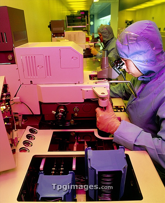
Fabrication of silicon-based integrated circuits (chips), showing a technician using a binocular microscope to check the alignment of a mask used in the photolithography stage of manufacture. Individual chips are constructed on a single wafer of crystalline silicon. The complicated pattern of embedded layers and zones which comprises each integrated circuit is created by successive imaging, etching and deposition or growth processes. Chips diced from the wafers being made here will be packaged in readiness for use as motor controllers in computer disk drives.
| px | px | dpi | = | cm | x | cm | = | MB |
Details
Creative#:
TOP06674338
Source:
達志影像
Authorization Type:
RM
Release Information:
須由TPG 完整授權
Model Release:
NO
Property Release:
NO
Right to Privacy:
No
Same folder images:
 Loading